Artem Voloskovets

AI models are consuming computing resources at a pace that increasingly challenges conventional semiconductor scaling. A new study published in Nature demonstrates a monolithic three-dimensional silicon architecture that increases transistor density through vertical integration rather than further miniaturization.
Building Up Instead of Shrinking Down

The semiconductor industry increased performance by shrinking transistors. Smaller components meant more transistors could fit onto a chip, allowing computing power to rise with each generation.
The new architecture follows a different path. Additional transistor layers increase density without requiring a proportional reduction in transistor dimensions. Researchers successfully stacked active silicon transistor layers while maintaining performance characteristics approaching those of advanced commercial devices.
AI Compute Growth Is Outrunning Traditional Chip Scaling
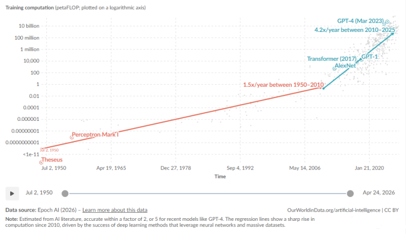
The second chart explains why the Nature research matters for AI rather than only for semiconductor engineering. From 1950 to 2010, the computation used to train notable AI systems grew at roughly 1.5× per year. That pace was already substantial, but it remained broadly aligned with improvements in computing hardware.
After 2010, the curve changed dramatically. According to the chart, training compute began increasing at approximately 4.2× per year, coinciding with the rise of deep learning. Systems such as AlexNet, GPT-1, GPT-3, and eventually GPT-4 moved rapidly up the compute scale. GPT-4 appears near the top of the chart, illustrating how far frontier AI models have moved from earlier milestones such as Deep Blue.
AI is no longer asking for incremental hardware improvements. It is demanding computational growth that increasingly exceeds the pace delivered by conventional semiconductor scaling. The gap between AI compute demand and semiconductor scaling has become a central topic across the AI hardware sector.
As AI models become larger, hardware designers are increasingly forced to search for new architectural solutions rather than relying exclusively on smaller manufacturing nodes.

What Researchers Actually Built
The Nature paper is not about a new processor, a new AI accelerator, or a new semiconductor material.
It describes a new manufacturing approach. Modern processors remain largely two-dimensional. Even advanced AI accelerators distribute logic, cache, memory controllers, and processing units across a flat silicon surface.
The researchers demonstrated a monolithic architecture containing three active transistor layers fabricated within a single structure. Unlike conventional 3D packaging, where separately manufactured chips are connected after production, monolithic integration creates active transistor layers during fabrication itself.
Key Technical Achievements:
- Three active silicon transistor layers stacked vertically
- Less than 10 nm layer-to-layer alignment error
- Manufacturing temperatures below 400°C
- Current densities exceeding 650 μA/μm
- Functional logic circuits
- Integrated SRAM memory structures
The reported current density above 650 μA/μm is particularly notable because many previous monolithic 3D approaches struggled to maintain transistor performance while stacking additional layers. Combined with sub-10 nm alignment accuracy and low-temperature processing, the results move the architecture closer to practical semiconductor manufacturing than many earlier demonstrations.
Processing temperature is one of the most important metrics in the study.
One of the biggest obstacles to monolithic 3D chips has been heat. Building additional transistor layers often requires temperatures high enough to damage circuitry that has already been fabricated underneath. The researchers addressed this issue using a low-temperature process compatible with existing semiconductor manufacturing constraints.
The study also demonstrated working SRAM memory and logic circuits inside the stacked architecture. That distinction matters because many experimental semiconductor technologies demonstrate individual components but fail to integrate memory and logic into a practical computing structure.
Raw Compute Is No Longer the Only Constraint
Semiconductor performance was measured largely by transistor counts and clock speeds. Large language models and multimodal systems have shifted attention toward memory bandwidth, latency and energy efficiency.
Semiconductor engineers often describe this bottleneck as the memory wall: processors can execute calculations faster than data can be delivered to them. Modern AI workloads require continuous movement of large volumes of data between memory and compute resources. As model sizes increase, memory access becomes a larger contributor to overall power consumption and system latency.
A vertically integrated architecture offers one potential solution. Placing memory resources closer to compute units reduces communication distance and may lower the amount of energy required to move information around the chip.
Why AI Hardware Needs New Architectures
| AI Hardware Challenge | Current Limitation | Potential Benefit of 3D Integration |
| Memory bandwidth | Long communication paths | Shorter data travel distances |
| Power consumption | High energy cost of data movement | Greater efficiency |
| Latency | Memory access delays | Faster communication |
| Chip density | Limited silicon area | More transistors per footprint |
| AI scaling | Rising infrastructure costs | Improved performance density |
Three-dimensional integration is increasingly viewed as a possible route to improving performance without relying exclusively on smaller process nodes.
Smartphones May Benefit Earlier Than Expected
The technology is often discussed in the context of AI infrastructure, but potential applications extend beyond hyperscale computing. Smartphone manufacturers are encountering similar limitations involving power consumption, heat and memory bandwidth.
Apple, Samsung, Qualcomm and MediaTek are all expanding on-device AI capabilities within strict battery, thermal and size constraints. Features such as real-time translation, image generation and local AI assistants require significantly more compute than previous generations of mobile software, increasing demand for denser and more efficient chip architectures.
Potential Advantages for Future Smartphones
- Faster on-device AI inference
- Lower battery consumption
- Reduced thermal output
- Larger local AI models
- More capable voice assistants
- Advanced image and video generation on-device
The smartphone industry may ultimately provide a clearer test case for monolithic 3D integration than AI data centers. Data-center operators can add more servers. Smartphone manufacturers do not have the same luxury. Every additional AI feature must fit inside a device whose battery, dimensions and thermal limits change only gradually from year to year.
The semiconductor industry spent decades increasing density by shrinking components. Vertical integration provides another mechanism for increasing transistor density when further miniaturization becomes increasingly difficult.
AI Data Centers Still Stand to Gain
Initial commercial deployment is more likely to target AI accelerators and high-performance computing systems than smartphones. Data-center operators can justify higher costs and adopt new semiconductor technologies faster than consumer device manufacturers.
Reducing data movement inside processors could improve efficiency at the system level. Even relatively small improvements become meaningful when multiplied across thousands of accelerators operating continuously inside AI clusters.
Could 3D Chips Reach Smartphones This Decade?
Commercial deployment remains uncertain. Historically, new semiconductor technologies have tended to appear first in high-performance computing systems before reaching consumer devices. Advanced packaging technologies, chiplet architectures and high-bandwidth memory followed a similar trajectory.
Monolithic 3D integration is likely to follow the same path. AI accelerators used in data centers would probably become the first large-scale commercial applications because they can justify higher manufacturing costs and adopt new technologies more quickly. For smartphone manufacturers, the appeal is straightforward: more AI capability without requiring larger batteries, thicker devices or substantially higher power consumption.
 Artem Voloskovets